Advanced x86. BIOS and System Management Mode Internals Reset Vector презентация

Содержание


Презентации» Информатика» Advanced x86. BIOS and System Management Mode Internals Reset Vector
Advanced x86: BIOS and System Management Mode Internals Reset VectorAll materials are licensed under a Creative Commons “Share Alike” license.
Reset Vector  Execution EnvironmentReal-Address Mode (Real Mode)
 The original x86 operating mode
 Referred toProcessor State After Reset
 EAX, EBX, ECX, EBP, ESI, EDI, ESPProcessor State After Reset:  Control Registers (CRs)
 Control registers CR2,Reset Vector
 At system reset, the an initial (“bootstrap”) processor beginsReset Vector Decoding
 Decoding (routing) is performed via decoders located inAside: Forensics People
 If the top of memory always contains aMini-Lab: BIOS Flash Decoding
 Let’s look at some of the decodingMini-Lab: BIOS Flash Decoding
 Offset D8-D9h is FWH_DEC_EN1
 As stated, thisMini-Lab: BIOS Flash Decoding
 Therefore, with FWH_DEC_EN bit 14 asserted, we’reMini-Lab: BIOS Flash DecodingMini-Lab: BIOS Flash Decoding
 Reset it back to 0xFFCC
 Couple ofMini-data-collection Lab: Reset Vector in BIOS Binary
 If we dump theReal Mode Memory
 16-bit operating mode
 Segmented memory model
 When operatingReal Mode Addressing: Segment Registers
 CS, DS, SS, ES, FS, GS
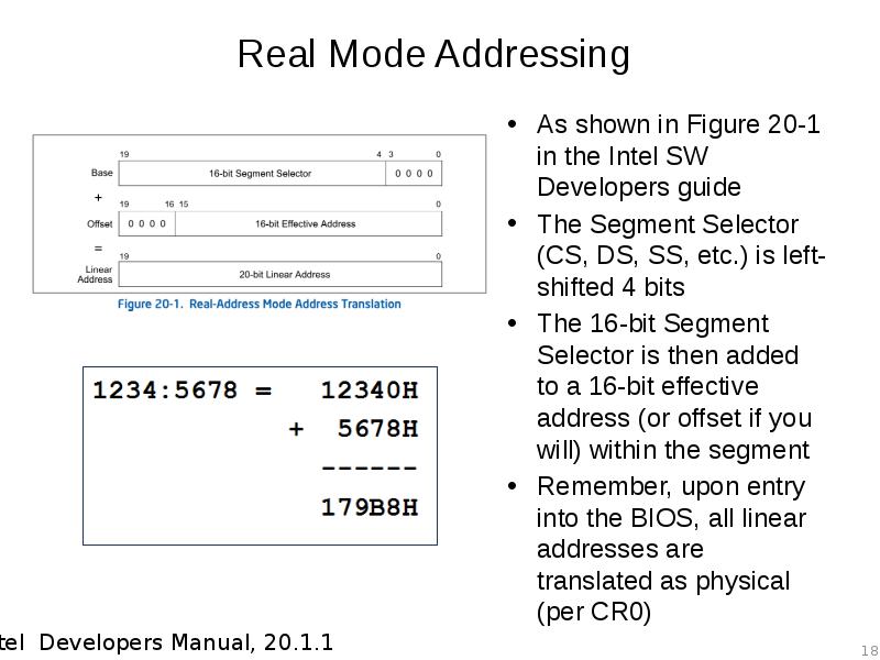
Real Mode Addressing
 As shown in Figure 20-1 in the IntelReal Mode Addressing Problem: Overlap
 Addresses in different segments can overlap
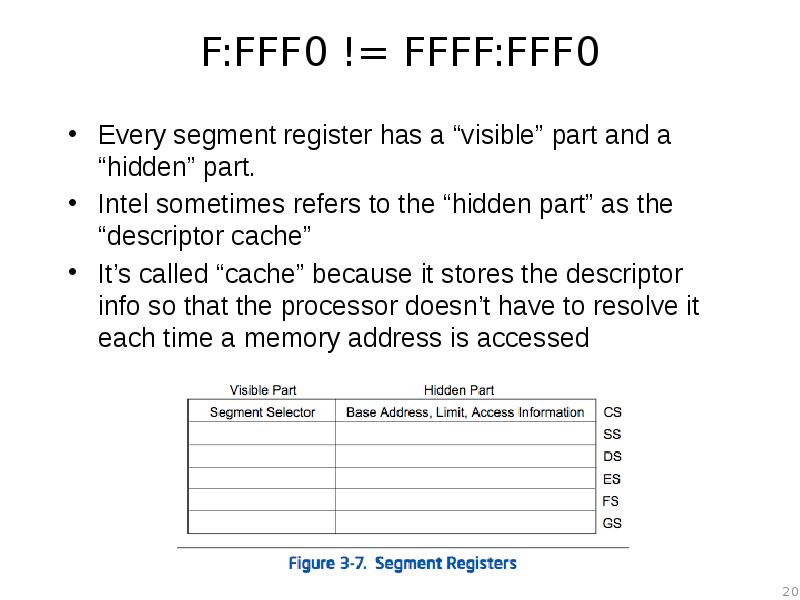
F:FFF0 != FFFF:FFF0
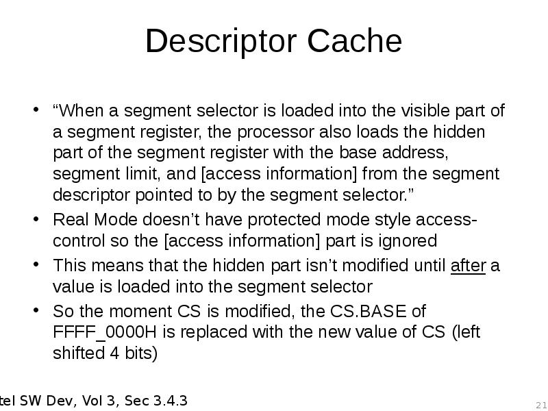
 Every segment register has a “visible” part andDescriptor Cache
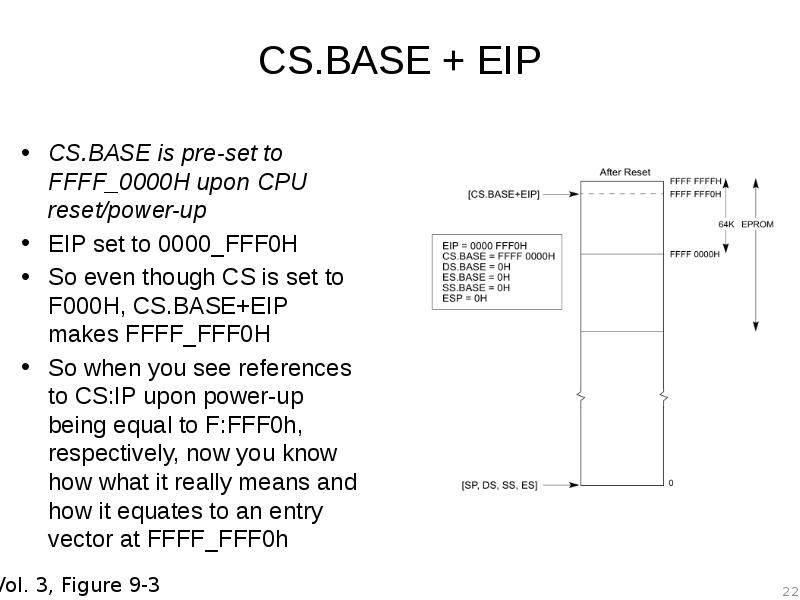
 “When a segment selector is loaded into the visibleCS.BASE + EIP
 CS.BASE is pre-set to FFFF_0000H upon CPU reset/power-up
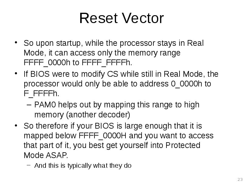
Reset Vector
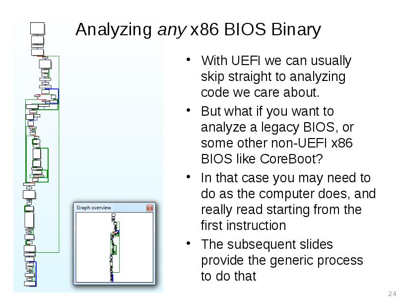
 So upon startup, while the processor stays in RealAnalyzing any x86 BIOS Binary
 With UEFI we can usually skipA dream deferred
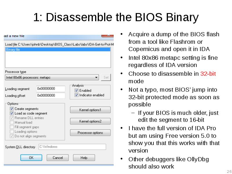
 We’re going to hold off on the rest1: Disassemble the BIOS Binary
 Acquire a dump of the BIOSFIXME
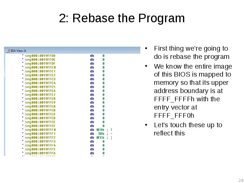
 Update procedure for new IDA demo 6.62: Rebase the Program
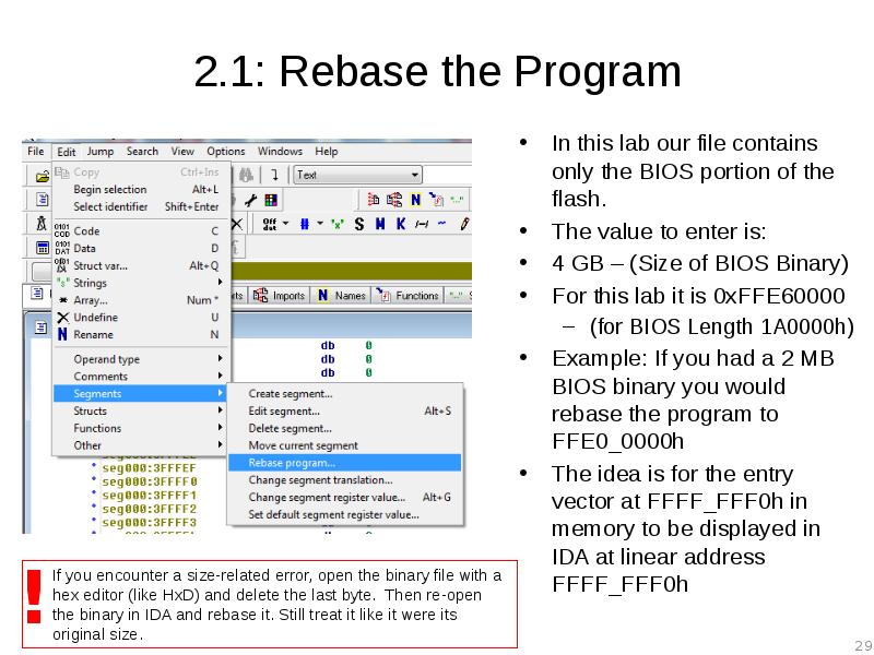
 First thing we’re going to do is2.1: Rebase the Program
 In this lab our file contains only2.2: Rebase the Program
 You know you have done it right3. Determine IDA Segments:  Manually Analyze the Reset Vector JMP
3.1: JMP rel16
 The address following our JMP instruction is FFFF_FFF3h3.2: Determine Segment Boundary
 So we know the destination of the4: Create Initial 16-bit Segment
 Edit –> Segments –> Create Segment
5: Identify Memory Model
 Once this segment is created, IDA “automagically”5.1: LGDT Instruction
 LGDT loads the values in the source operand5.2: Import GDT/IDT Structures
 You can import these structures into IDA5.3: Define GdtPtr
 Go to the address referenced by the operand5.4: Define GDT Entries
 We know it’s location is in our5.5: Full GDT
 The GdtEntry structure definition in peewee.h can be5.5: Full GDT
 Here is the entire GDT for reference. You6: Create the 32-bit BIOS segment
 Now create the 32-bit segment
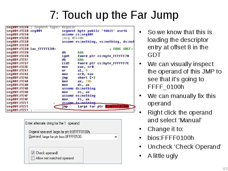
7: Touch up the Far Jump
 So we know that thisWelcome to BIOS Analysis
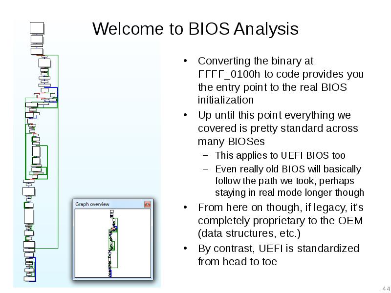
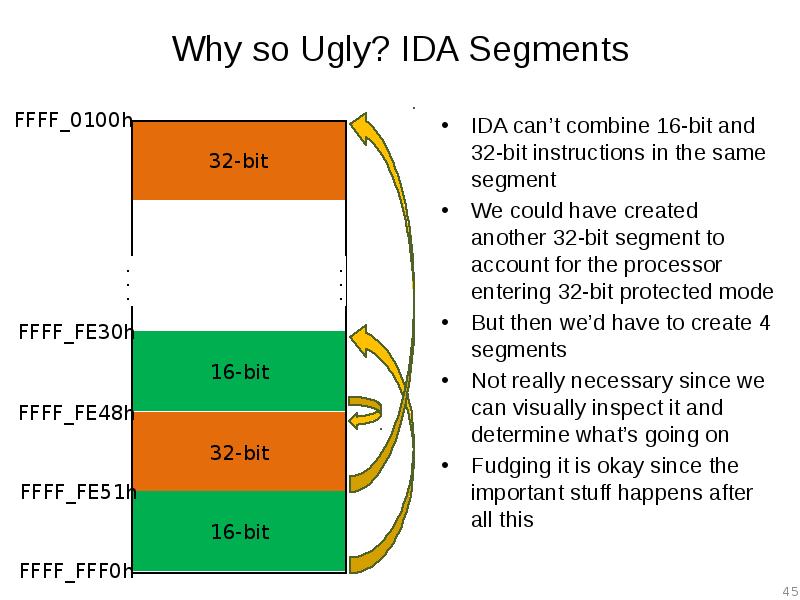
 Converting the binary at FFFF_0100h to codeWhy so Ugly? IDA Segments
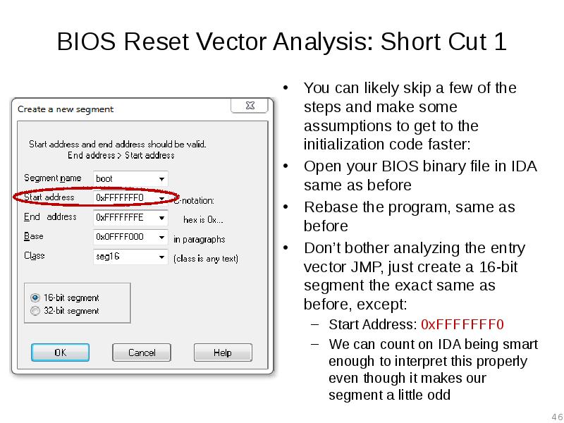
 IDA can’t combine 16-bit and 32-bitBIOS Reset Vector Analysis: Short Cut 1
 You can likely skipBIOS Reset Vector Analysis: Short Cut 2
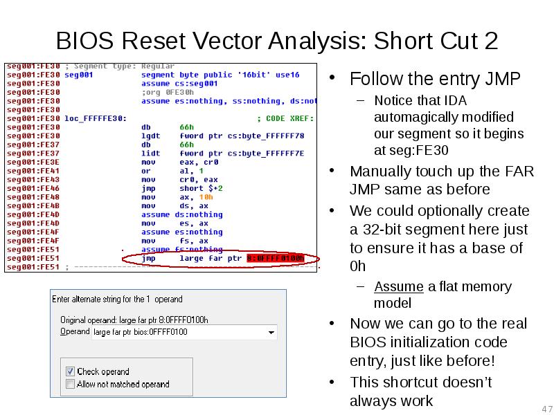
 Follow the entry JMP
Lab: Scratch the surface
 Repeat the process we just did for


Слайды и текст этой презентации
Слайд 1
Описание слайда:
Advanced x86: BIOS and System Management Mode Internals Reset Vector


Слайд 2
Описание слайда:
All materials are licensed under a Creative Commons “Share Alike” license. http://creativecommons.org/licenses/by-sa/3.0/

Слайд 3
Описание слайда:
Reset Vector Execution Environment

Слайд 4
Описание слайда:
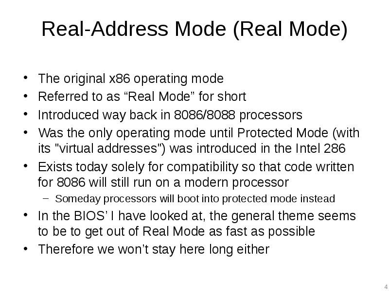
Real-Address Mode (Real Mode) The original x86 operating mode Referred to as “Real Mode” for short Introduced way back in 8086/8088 processors Was the only operating mode until Protected Mode (with its "virtual addresses") was introduced in the Intel 286 Exists today solely for compatibility so that code written for 8086 will still run on a modern processor Someday processors will boot into protected mode instead In the BIOS’ I have looked at, the general theme seems to be to get out of Real Mode as fast as possible Therefore we won’t stay here long either

Слайд 5
Описание слайда:
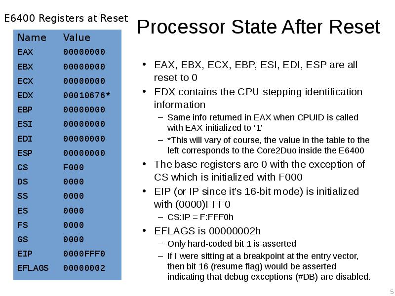
Processor State After Reset EAX, EBX, ECX, EBP, ESI, EDI, ESP are all reset to 0 EDX contains the CPU stepping identification information Same info returned in EAX when CPUID is called with EAX initialized to ‘1’ *This will vary of course, the value in the table to the left corresponds to the Core2Duo inside the E6400 The base registers are 0 with the exception of CS which is initialized with F000 EIP (or IP since it’s 16-bit mode) is initialized with (0000)FFF0 CS:IP = F:FFF0h EFLAGS is 00000002h Only hard-coded bit 1 is asserted If I were sitting at a breakpoint at the entry vector, then bit 16 (resume flag) would be asserted indicating that debug exceptions (#DB) are disabled.

Слайд 6
Описание слайда:
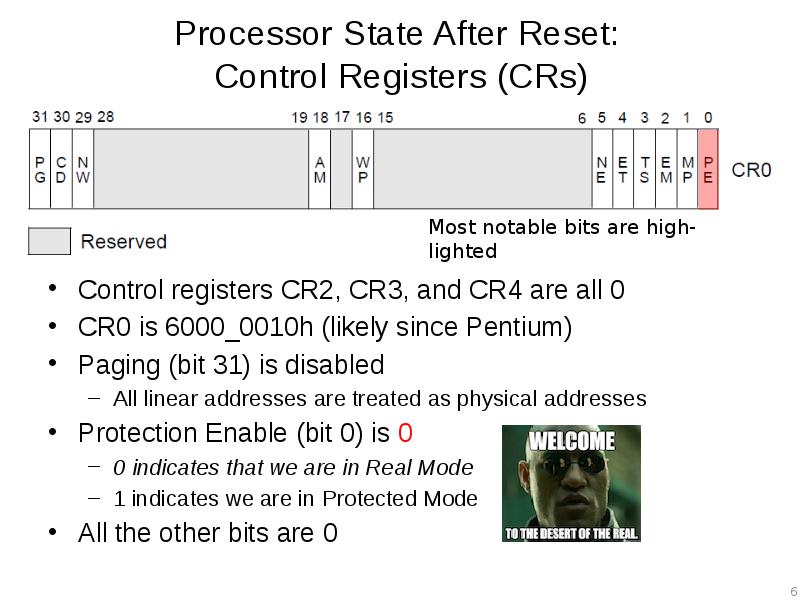
Processor State After Reset: Control Registers (CRs) Control registers CR2, CR3, and CR4 are all 0 CR0 is 6000_0010h (likely since Pentium) Paging (bit 31) is disabled All linear addresses are treated as physical addresses Protection Enable (bit 0) is 0 0 indicates that we are in Real Mode 1 indicates we are in Protected Mode All the other bits are 0

Слайд 7
Описание слайда:
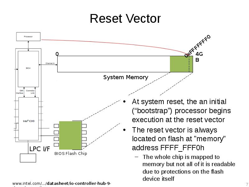
Reset Vector At system reset, the an initial (“bootstrap”) processor begins execution at the reset vector The reset vector is always located on flash at "memory" address FFFF_FFF0h The whole chip is mapped to memory but not all of it is readable due to protections on the flash device itself

Слайд 8
Описание слайда:
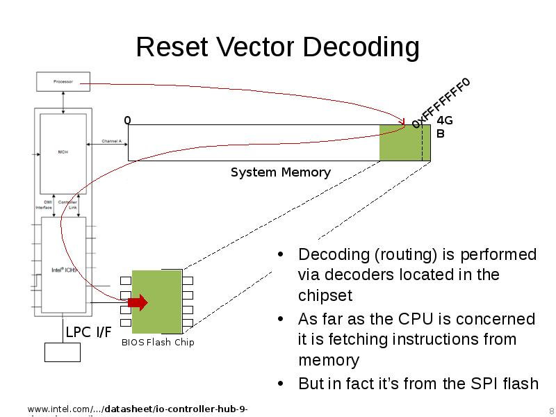
Reset Vector Decoding Decoding (routing) is performed via decoders located in the chipset As far as the CPU is concerned it is fetching instructions from memory But in fact it’s from the SPI flash

Слайд 9
Описание слайда:
Aside: Forensics People If the top of memory always contains a memory-mapped copy of part of the SPI flash chip, that means it should theoretically show up in memory forensic dumps (e.g. those given out by memory forensic challenges) I’ve never had time to test this, but you should see if you can go grab some memory forensics dumps and determine whether there is a complete copy of the BIOS in the memory dump, or only a partial copy (and if partial, where it ends) Probably should start by testing on a system you have known BIOS dump for As I mentioned before, virtual machines have virtual BIOSes, so you could also determine if the dump was taken off a virtual machine by comparing against some virtual BIOSes Let me know what you find! :) A volatility plugin to carve BIOS out of memdumps would be cool  IIRC someone might have done this now, but I can’t find the link again…

Слайд 10
Описание слайда:
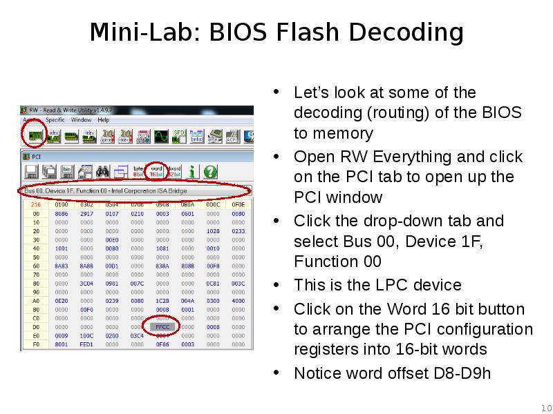
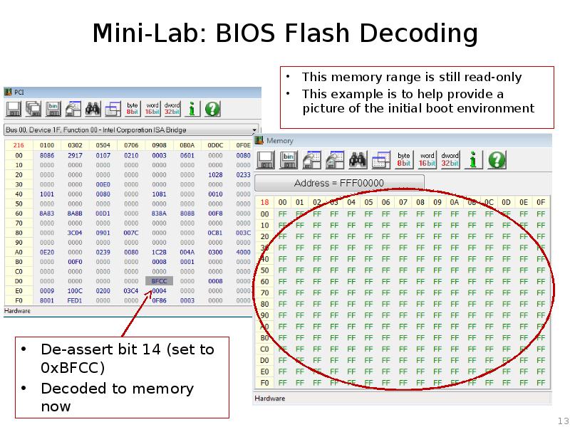
Mini-Lab: BIOS Flash Decoding Let’s look at some of the decoding (routing) of the BIOS to memory Open RW Everything and click on the PCI tab to open up the PCI window Click the drop-down tab and select Bus 00, Device 1F, Function 00 This is the LPC device Click on the Word 16 bit button to arrange the PCI configuration registers into 16-bit words Notice word offset D8-D9h

Слайд 11
Описание слайда:
Mini-Lab: BIOS Flash Decoding Offset D8-D9h is FWH_DEC_EN1 As stated, this controls the decoding of ranges to the FWH If your system uses SPI and not a Firmware Hub (and it does since FWH is very rare), it still decodes to the SPI BIOS We want bit 14 which decodes FFF0_0000h – FFF7_FFFFh

Слайд 12
Описание слайда:
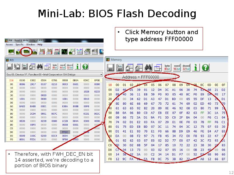
Mini-Lab: BIOS Flash Decoding Therefore, with FWH_DEC_EN bit 14 asserted, we’re decoding to a portion of BIOS binary

Слайд 13
Описание слайда:
Mini-Lab: BIOS Flash Decoding

Слайд 14
Описание слайда:
Mini-Lab: BIOS Flash Decoding Reset it back to 0xFFCC Couple of notes: Your original values may differ since BIOS flips them on and off as the developers decided necessary Bit 15 is Read Only and always asserted

Слайд 15
Описание слайда:
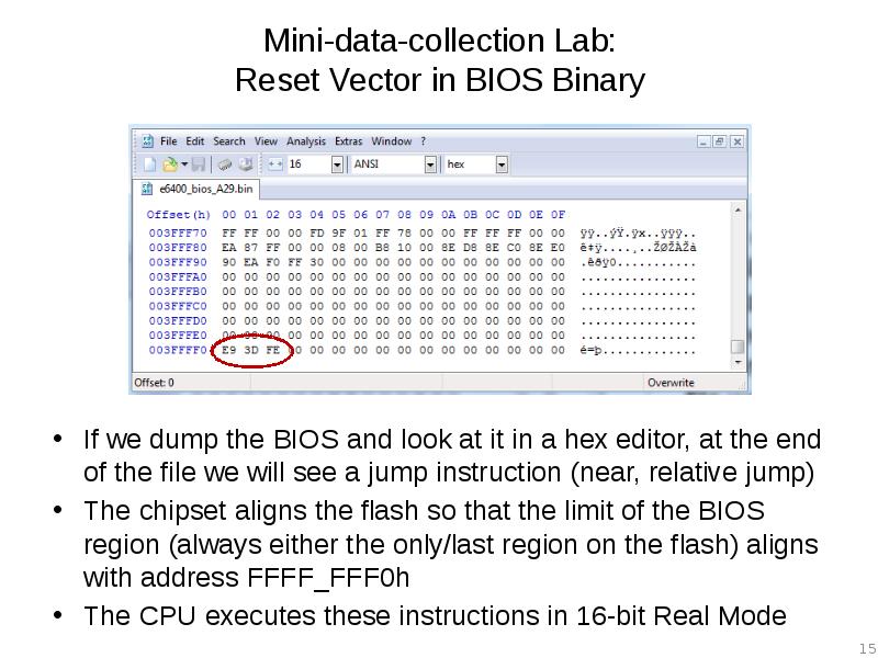
Mini-data-collection Lab: Reset Vector in BIOS Binary If we dump the BIOS and look at it in a hex editor, at the end of the file we will see a jump instruction (near, relative jump) The chipset aligns the flash so that the limit of the BIOS region (always either the only/last region on the flash) aligns with address FFFF_FFF0h The CPU executes these instructions in 16-bit Real Mode

Слайд 16
Описание слайда:
Real Mode Memory 16-bit operating mode Segmented memory model When operating in real-address mode, the default addressing and operand size is 16 bits An address-size override can be used in real-address mode to enable access to 32-bit addressing (like the extended general-purpose registers EAX, EDX, etc.) However, the maximum allowable 32-bit linear address is still 000F_FFFFH (220 -1) So how can it address FFFF_FFF0h? We’ll answer that in a bit

Слайд 17
Описание слайда:
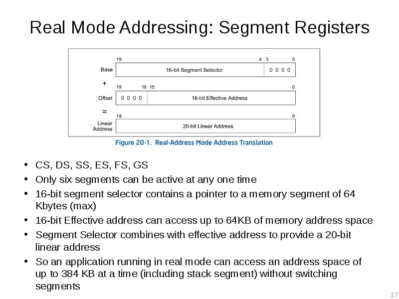
Real Mode Addressing: Segment Registers CS, DS, SS, ES, FS, GS Only six segments can be active at any one time 16-bit segment selector contains a pointer to a memory segment of 64 Kbytes (max) 16-bit Effective address can access up to 64KB of memory address space Segment Selector combines with effective address to provide a 20-bit linear address So an application running in real mode can access an address space of up to 384 KB at a time (including stack segment) without switching segments

Слайд 18
Описание слайда:
Real Mode Addressing As shown in Figure 20-1 in the Intel SW Developers guide The Segment Selector (CS, DS, SS, etc.) is left-shifted 4 bits The 16-bit Segment Selector is then added to a 16-bit effective address (or offset if you will) within the segment Remember, upon entry into the BIOS, all linear addresses are translated as physical (per CR0)

Слайд 19
Описание слайда:
Real Mode Addressing Problem: Overlap Addresses in different segments can overlap Given such a limited environment it’s no wonder we want to choose a different operating mode as soon as possible

Слайд 20
Описание слайда:
F:FFF0 != FFFF:FFF0 Every segment register has a “visible” part and a “hidden” part. Intel sometimes refers to the “hidden part” as the “descriptor cache” It’s called “cache” because it stores the descriptor info so that the processor doesn’t have to resolve it each time a memory address is accessed

Слайд 21
Описание слайда:
Descriptor Cache “When a segment selector is loaded into the visible part of a segment register, the processor also loads the hidden part of the segment register with the base address, segment limit, and [access information] from the segment descriptor pointed to by the segment selector.” Real Mode doesn’t have protected mode style access-control so the [access information] part is ignored This means that the hidden part isn’t modified until after a value is loaded into the segment selector So the moment CS is modified, the CS.BASE of FFFF_0000H is replaced with the new value of CS (left shifted 4 bits)

Слайд 22
Описание слайда:
CS.BASE + EIP CS.BASE is pre-set to FFFF_0000H upon CPU reset/power-up EIP set to 0000_FFF0H So even though CS is set to F000H, CS.BASE+EIP makes FFFF_FFF0H So when you see references to CS:IP upon power-up being equal to F:FFF0h, respectively, now you know how what it really means and how it equates to an entry vector at FFFF_FFF0h

Слайд 23
Описание слайда:
Reset Vector So upon startup, while the processor stays in Real Mode, it can access only the memory range FFFF_0000h to FFFF_FFFFh. If BIOS were to modify CS while still in Real Mode, the processor would only be able to address 0_0000h to F_FFFFh. PAM0 helps out by mapping this range to high memory (another decoder) So therefore if your BIOS is large enough that it is mapped below FFFF_0000H and you want to access that part of it, you best get yourself into Protected Mode ASAP. And this is typically what they do

Слайд 24
Описание слайда:
Analyzing any x86 BIOS Binary With UEFI we can usually skip straight to analyzing code we care about. But what if you want to analyze a legacy BIOS, or some other non-UEFI x86 BIOS like CoreBoot? In that case you may need to do as the computer does, and really read starting from the first instruction The subsequent slides provide the generic process to do that

Слайд 25
Описание слайда:
A dream deferred We’re going to hold off on the rest of the entry vector analysis for now, and go back to it later if we have time. We never have time ;) I left the slides in here for if you want to try to go through an equivalent process Note: I know the slides are a little hard to follow and occasionally make jumps in intuition. I’ve been wanting to clean these up from John’s version, but haven’t had time

Слайд 26
Описание слайда:
1: Disassemble the BIOS Binary Acquire a dump of the BIOS flash from a tool like Flashrom or Copernicus and open it in IDA Intel 80x86 metapc setting is fine regardless of IDA version Choose to disassemble in 32-bit mode Not a typo, most BIOS’ jump into 32-bit protected mode as soon as possible If your BIOS is much older, just edit the segment to 16-bit I have the full version of IDA Pro but am using Free version 5.0 to show you that this works with that version Other debuggers like OllyDbg should also work

Слайд 27
Описание слайда:
FIXME Update procedure for new IDA demo 6.6

Слайд 28
Описание слайда:
2: Rebase the Program First thing we’re going to do is rebase the program We know the entire image of this BIOS is mapped to memory so that its upper address boundary is at FFFF_FFFFh with the entry vector at FFFF_FFF0h Let’s touch these up to reflect this

Слайд 29
Описание слайда:
2.1: Rebase the Program In this lab our file contains only the BIOS portion of the flash. The value to enter is: 4 GB – (Size of BIOS Binary) For this lab it is 0xFFE60000 (for BIOS Length 1A0000h) Example: If you had a 2 MB BIOS binary you would rebase the program to FFE0_0000h The idea is for the entry vector at FFFF_FFF0h in memory to be displayed in IDA at linear address FFFF_FFF0h

Слайд 30
Описание слайда:
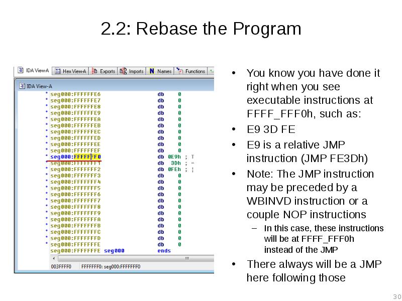
2.2: Rebase the Program You know you have done it right when you see executable instructions at FFFF_FFF0h, such as: E9 3D FE E9 is a relative JMP instruction (JMP FE3Dh) Note: The JMP instruction may be preceded by a WBINVD instruction or a couple NOP instructions In this case, these instructions will be at FFFF_FFF0h instead of the JMP There always will be a JMP here following those

Слайд 31
Описание слайда:
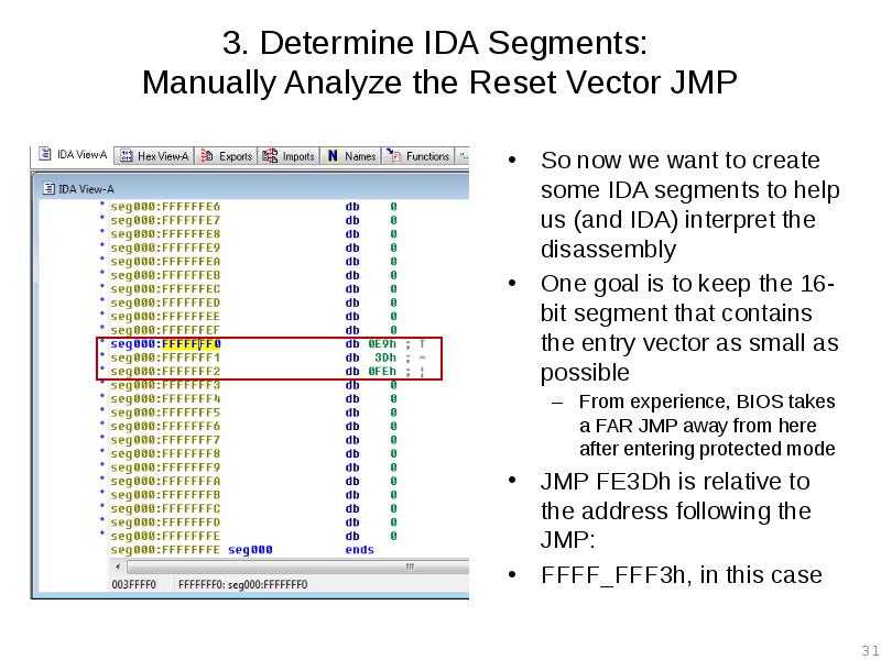
3. Determine IDA Segments: Manually Analyze the Reset Vector JMP So now we want to create some IDA segments to help us (and IDA) interpret the disassembly One goal is to keep the 16-bit segment that contains the entry vector as small as possible From experience, BIOS takes a FAR JMP away from here after entering protected mode JMP FE3Dh is relative to the address following the JMP: FFFF_FFF3h, in this case

Слайд 32
Описание слайда:
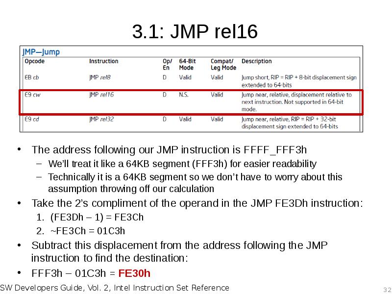
3.1: JMP rel16 The address following our JMP instruction is FFFF_FFF3h We’ll treat it like a 64KB segment (FFF3h) for easier readability Technically it is a 64KB segment so we don’t have to worry about this assumption throwing off our calculation Take the 2’s compliment of the operand in the JMP FE3Dh instruction: (FE3Dh – 1) = FE3Ch ~FE3Ch = 01C3h Subtract this displacement from the address following the JMP instruction to find the destination: FFF3h – 01C3h = FE30h

Слайд 33
Описание слайда:
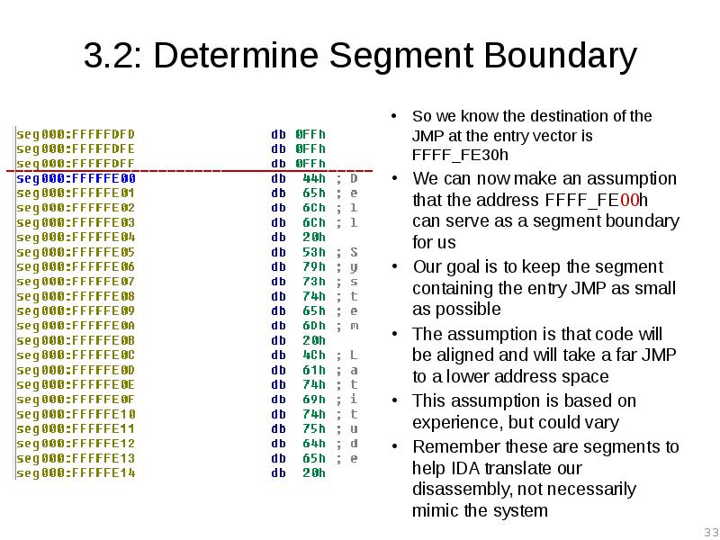
3.2: Determine Segment Boundary So we know the destination of the JMP at the entry vector is FFFF_FE30h We can now make an assumption that the address FFFF_FE00h can serve as a segment boundary for us Our goal is to keep the segment containing the entry JMP as small as possible The assumption is that code will be aligned and will take a far JMP to a lower address space This assumption is based on experience, but could vary Remember these are segments to help IDA translate our disassembly, not necessarily mimic the system

Слайд 34
Описание слайда:
4: Create Initial 16-bit Segment Edit –> Segments –> Create Segment Pick any segment name you want Class can be any text name 16-bit segment Start Address = 0xFFFFFE00 End Address = 0xFFFFFFFE Remember: IDA Does not like the address FFFFFFFF (-1) !! Actually, according to IDA documentation, the 32-bit version of IDA doesn’t “like” any address at or above FF00_0000h  Base = 0x0FFFF000 CS.BASE = FFFF_0000h on boot

Слайд 35
Описание слайда:
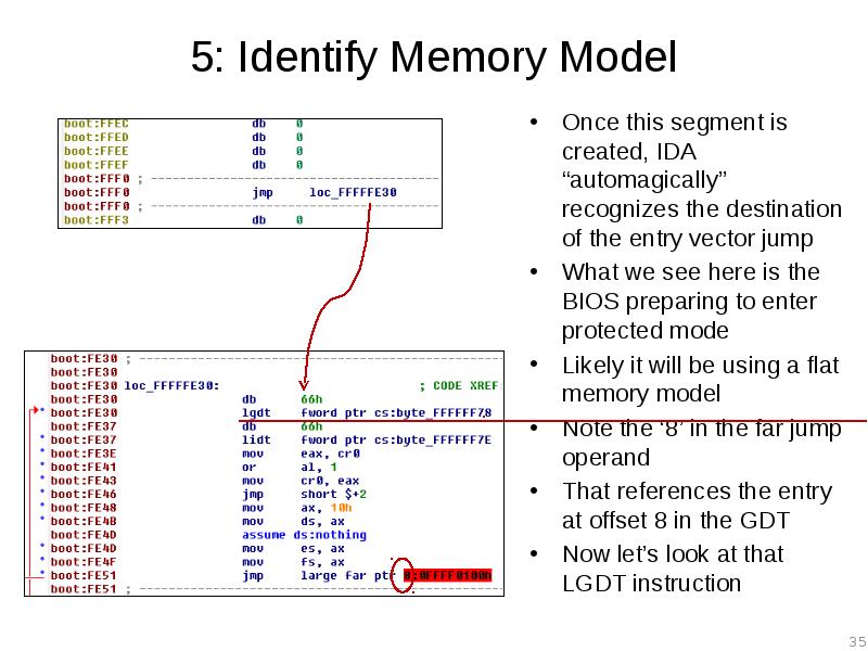
5: Identify Memory Model Once this segment is created, IDA “automagically” recognizes the destination of the entry vector jump What we see here is the BIOS preparing to enter protected mode Likely it will be using a flat memory model Note the ‘8’ in the far jump operand That references the entry at offset 8 in the GDT Now let’s look at that LGDT instruction

Слайд 36
Описание слайда:
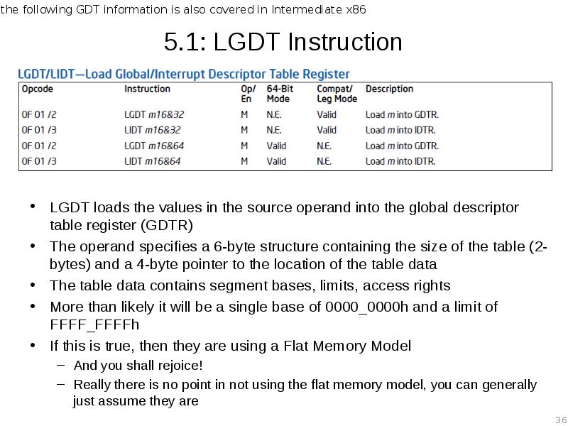
5.1: LGDT Instruction LGDT loads the values in the source operand into the global descriptor table register (GDTR) The operand specifies a 6-byte structure containing the size of the table (2-bytes) and a 4-byte pointer to the location of the table data The table data contains segment bases, limits, access rights More than likely it will be a single base of 0000_0000h and a limit of FFFF_FFFFh If this is true, then they are using a Flat Memory Model And you shall rejoice! Really there is no point in not using the flat memory model, you can generally just assume they are

Слайд 37
Описание слайда:
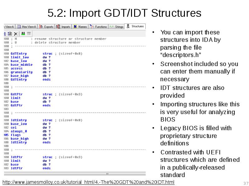
5.2: Import GDT/IDT Structures You can import these structures into IDA by parsing the file “descriptors.h” Screenshot included so you can enter them manually if necessary IDT structures are also provided Importing structures like this is very useful for analyzing BIOS Legacy BIOS is filled with proprietary structure definitions Contrasted with UEFI structures which are defined in a publically-released standard

Слайд 38
Описание слайда:
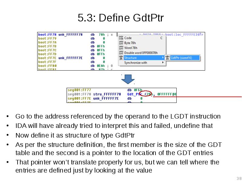
5.3: Define GdtPtr Go to the address referenced by the operand to the LGDT instruction IDA will have already tried to interpret this and failed, undefine that Now define it as structure of type GdtPtr As per the structure definition, the first member is the size of the GDT table and the second is a pointer to the location of the GDT entries That pointer won’t translate properly for us, but we can tell where the entries are defined just by looking at the value

Слайд 39
Описание слайда:
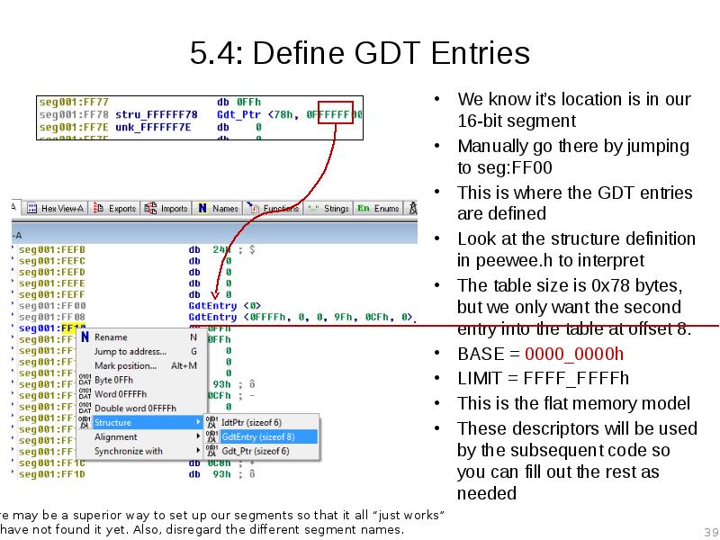
5.4: Define GDT Entries We know it’s location is in our 16-bit segment Manually go there by jumping to seg:FF00 This is where the GDT entries are defined Look at the structure definition in peewee.h to interpret The table size is 0x78 bytes, but we only want the second entry into the table at offset 8: BASE = 0000_0000h LIMIT = FFFF_FFFFh This is the flat memory model These descriptors will be used by the subsequent code so you can fill out the rest as needed

Слайд 40
Описание слайда:
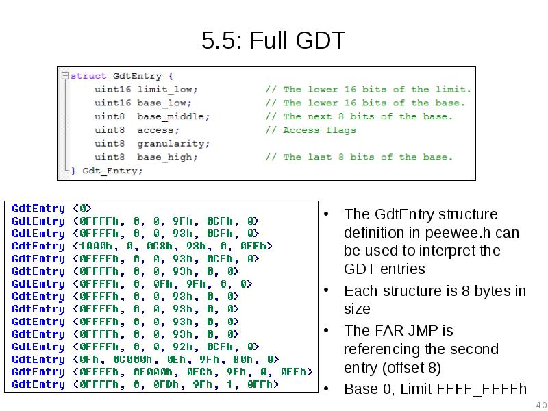
5.5: Full GDT The GdtEntry structure definition in peewee.h can be used to interpret the GDT entries Each structure is 8 bytes in size The FAR JMP is referencing the second entry (offset 8) Base 0, Limit FFFF_FFFFh

Слайд 41
Описание слайда:
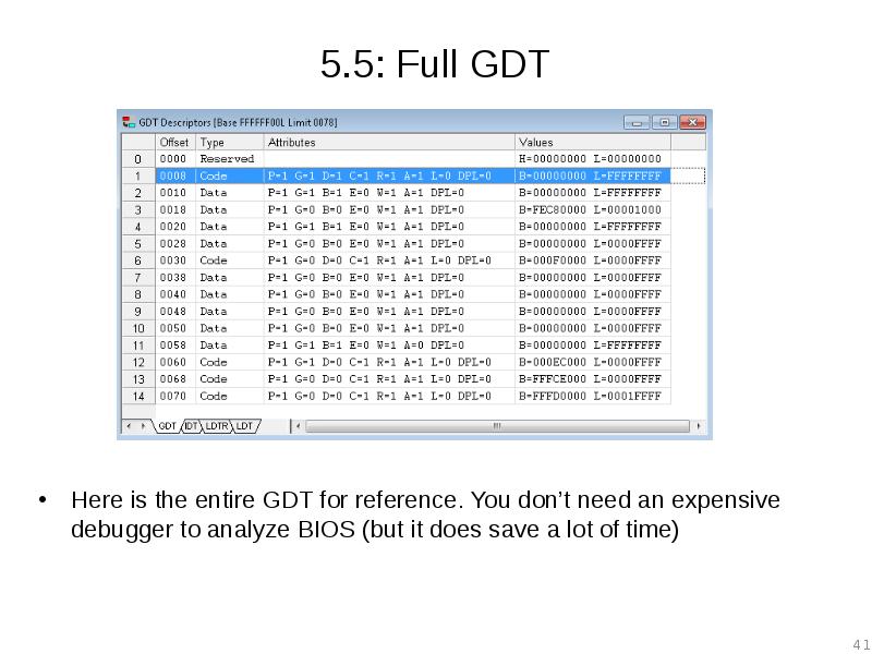
5.5: Full GDT Here is the entire GDT for reference. You don’t need an expensive debugger to analyze BIOS (but it does save a lot of time)

Слайд 42
Описание слайда:
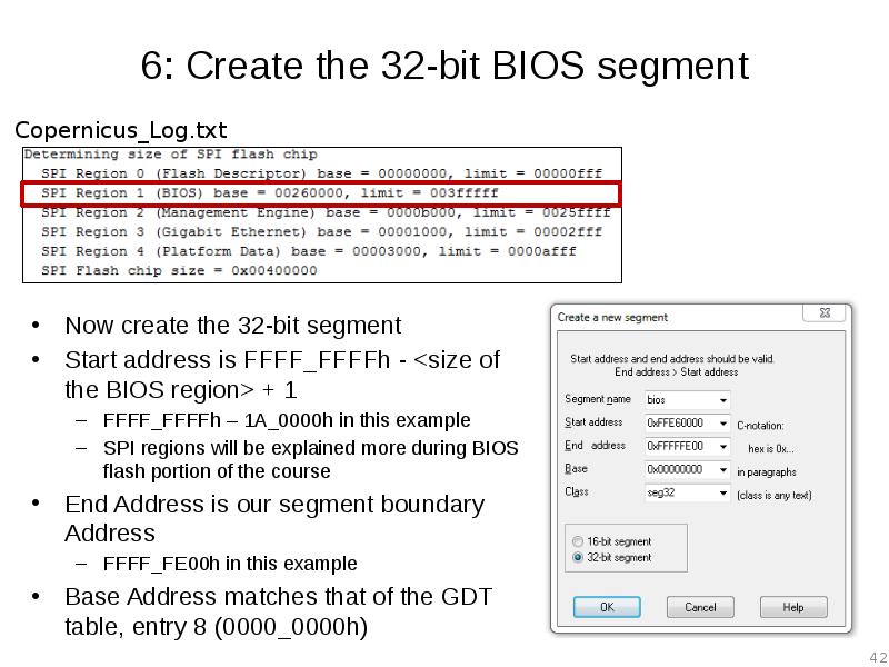
6: Create the 32-bit BIOS segment Now create the 32-bit segment Start address is FFFF_FFFFh - <size of the BIOS region> + 1 FFFF_FFFFh – 1A_0000h in this example SPI regions will be explained more during BIOS flash portion of the course End Address is our segment boundary Address FFFF_FE00h in this example Base Address matches that of the GDT table, entry 8 (0000_0000h)

Слайд 43
Описание слайда:
7: Touch up the Far Jump So we know that this is loading the descriptor entry at offset 8 in the GDT We can visually inspect the operand of this JMP to see that it’s going to FFFF_0100h We can manually fix this operand Right click the operand and select ‘Manual’ Change it to: bios:FFFF0100h Uncheck ‘Check Operand’ A little ugly

Слайд 44
Описание слайда:
Welcome to BIOS Analysis Converting the binary at FFFF_0100h to code provides you the entry point to the real BIOS initialization Up until this point everything we covered is pretty standard across many BIOSes This applies to UEFI BIOS too Even really old BIOS will basically follow the path we took, perhaps staying in real mode longer though From here on though, if legacy, it’s completely proprietary to the OEM (data structures, etc.) By contrast, UEFI is standardized from head to toe

Слайд 45
Описание слайда:
Why so Ugly? IDA Segments IDA can’t combine 16-bit and 32-bit instructions in the same segment We could have created another 32-bit segment to account for the processor entering 32-bit protected mode But then we’d have to create 4 segments Not really necessary since we can visually inspect it and determine what’s going on Fudging it is okay since the important stuff happens after all this

Слайд 46
Описание слайда:
BIOS Reset Vector Analysis: Short Cut 1 You can likely skip a few of the steps and make some assumptions to get to the initialization code faster: Open your BIOS binary file in IDA same as before Rebase the program, same as before Don’t bother analyzing the entry vector JMP, just create a 16-bit segment the exact same as before, except: Start Address: 0xFFFFFFF0 We can count on IDA being smart enough to interpret this properly even though it makes our segment a little odd

Слайд 47
Описание слайда:
BIOS Reset Vector Analysis: Short Cut 2 Follow the entry JMP Notice that IDA automagically modified our segment so it begins at seg:FE30 Manually touch up the FAR JMP same as before We could optionally create a 32-bit segment here just to ensure it has a base of 0h Assume a flat memory model Now we can go to the real BIOS initialization code entry, just like before! This shortcut doesn’t always work

Слайд 48
Описание слайда:
Lab: Scratch the surface Repeat the process we just did for the E6400 BIOS on each of your BIOS dumps We'll see if there are any where it leads to early confusion


Скачать презентацию на тему Advanced x86. BIOS and System Management Mode Internals Reset Vector можно ниже:
Похожие презентации